Multi Nano Sense Targets a Compact MEMS Gas Sensor and Readout Chip
The Nagpur company’s new development programme combines a MEMS sensing element with a custom analogue front end. Sub-200-millisecond response and a compact package are targets, with testing and scale-up still ahead.
A gas sensor has to do more than detect a change in its surroundings: it must turn that change into a dependable electrical measurement. A new programme at Nagpur-based Multi Nano Sense Technologies aims to bring the sensing element and its electronic readout into a compact, integrated platform.
The Technology Development Board announced an agreement with the company on 29 September 2026. It provides ₹37.51 crore in support through optionally convertible debt towards a ₹75.02-crore project. The technical objective is to move the platform from technology readiness level 4 to level 9, an intended progression that still requires development, validation and scale-up.
Pairing the sensor with its signal-processing chip
The official release describes a MEMS TCDIR sensing element coupled to a CMOS application-specific analogue-front-end system-on-chip. MEMS refers to micro-electromechanical systems; the analogue front end acquires and processes the sensing element’s signal. Integrating these functions is central to the proposed platform, rather than merely shrinking an enclosure around existing instruments.
The programme targets a package smaller than 25 × 25 × 15 millimetres and a response time below 200 milliseconds. These are development specifications in the announcement, not independently reported results from a finished product. The release also identifies automatic calibration, environmental compensation and a software gas library as planned capabilities.
Multi Nano Sense’s existing platform description discusses CMOS-MEMS and other MEMS approaches, with an emphasis on size, power use and gas selectivity. That broader company description supplies context; it does not validate the performance of this newly supported design.
The difficult part is a reliable measurement
Leak detection, industrial process control and health-and-safety monitoring are among the applications identified by the board. Hydrogen systems and battery-related uses are also mentioned as potential markets. Different applications create different demands on sensitivity, selectivity and response under changing conditions.
For that reason, the eventual test evidence will matter as much as the package dimensions. The announcement does not provide detection limits for individual gases, cross-sensitivity measurements, power-consumption figures or long-duration calibration data. Environmental compensation is a proposed capability, not proof that temperature and humidity effects have already been eliminated.
The development is significant for India’s sensor and semiconductor ecosystem because it joins a sensing device with a purpose-built readout chip. The next substantive milestone will be validated performance for specified gases and operating conditions, followed by evidence that manufacturing can reproduce that performance consistently.
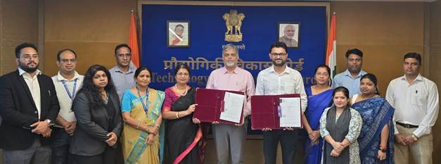
Image: participants displaying documents at the Technology Development Board agreement event. Credit: TDB / DST / PIB Delhi. This is an event photograph, not an image of the proposed sensor.