IIT Delhi Builds India's First Indigenous Micro-GPU, Charts a Path to 65nm Silicon
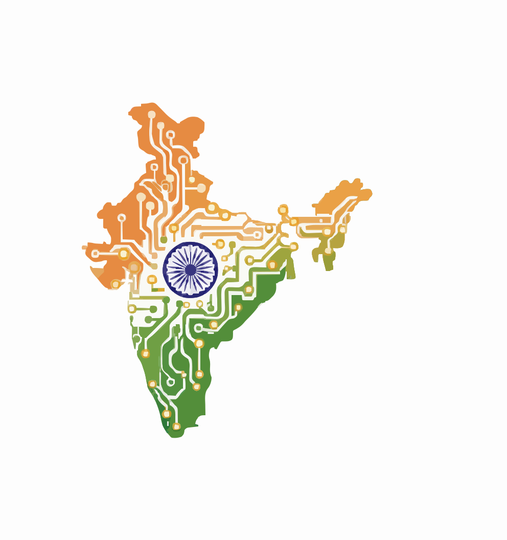
IIT Delhi researchers have demonstrated an indigenously designed micro-GPU running on an FPGA, with a roadmap to a multi-core design, a compiler toolchain and a 65nm ASIC. It is a small but concrete step towards home-grown graphics silicon for India's embedded electronics.

For decades, graphics processors have been one of the most conspicuous gaps in India's electronics supply chain. Every GPU in an Indian phone, car dashboard, factory control panel or AI server is designed abroad, and almost always manufactured abroad too. A small but symbolically important project out of IIT Delhi now claims a first step towards changing that.
What IIT Delhi announced
Researchers in the Electrical Engineering Department at IIT Delhi have developed what the institute describes as India's first working, demonstrable, indigenously designed micro Graphics Processing Unit (micro-GPU) built by a university. The announcement was made on 24 September 2026 and has since been reported by Business Standard, Swarajya and other outlets.
The work was carried out by M.Tech students Nammi Akash and M. Ravi Teja, under the guidance of Prof. Jayadeva and Prof. Kaushik Saha.
At its core is a custom floating-point GPU engine, written entirely at the register-transfer level (RTL) — the hardware-description layer at which chip logic is designed before it is turned into silicon. The team has mapped that design onto a Xilinx Spartan-7 FPGA (field programmable gate array) and used it to demonstrate programmable graphics rendering.
In other words, this is not yet a fabricated chip. It is a complete, working processor design running on reconfigurable hardware, which is the standard proving ground before a design is committed to an expensive silicon tape-out.
Why a "micro" GPU matters
It is important to be precise about what has been built. The IIT Delhi design is not a competitor to the data-centre GPUs used to train large AI models. The team positions it as a scalable, programmable graphics-processor IP block for low-cost embedded visualisation. The applications it lists include:
- industrial control displays and low-cost human-machine interfaces;
- dashboard navigators for e-rickshaws;
- inland-water navigation terminals for small fishing boats;
- educational e-book readers and other affordable embedded devices.
These are exactly the kinds of high-volume, price-sensitive products where India's domestic electronics manufacturing is growing fastest — and where the graphics silicon is currently imported. Business Standard, reporting on the announcement, noted that GPUs are now used widely across modern hardware, including AI and machine-learning engines, and that currently all GPUs used in India are imported.
The researchers have said their aim is a compact but programmable graphics architecture that works on FPGAs today and can eventually be manufactured as an ASIC (application-specific integrated circuit). They have also framed the effort in terms of digital access: affordable, locally designed display hardware could lower the cost of devices aimed at under-served users.
The roadmap: from FPGA to 65nm silicon
The team has laid out a staged plan. The next steps include:
- A multi-core design — an 8–16-core, vector-style graphics processor architecture.
- A software stack — an optimised compiler and graphics software toolchain, without which no GPU is usable by product developers.
- Silicon — a proof-of-concept implementation on a 65nm ASIC process.
The choice of 65nm is pragmatic. It is a mature node, far from the leading edge, but it is inexpensive, well-understood and appropriate for embedded display controllers. It is also the kind of node that is realistic for academic tape-outs through government-supported multi-project wafer programmes.
The toolchain step deserves emphasis. Much of the value — and the lock-in — of commercial GPUs lies in their software ecosystems. An indigenous graphics IP that ships with its own compiler and drivers is far more likely to be adopted by Indian device makers than a bare hardware block.
Getting to that point is not trivial for an academic team. Moving from an FPGA prototype to an ASIC requires physical design, verification against manufacturing rules and access to foundry process kits, all of which cost time and money. How the team funds and schedules that step will be the clearest signal of whether the micro-GPU is on a path to a product or remains a research demonstrator.
How it fits into India's chip push
The announcement lands a week after SEMICON India 2026 in New Delhi, where the government and industry showcased progress on fabs, assembly-and-test plants and design programmes. Most of the headline investments in India's semiconductor mission have gone into manufacturing capacity — fabs and OSAT (outsourced semiconductor assembly and test) facilities. Design capability, and specifically indigenous processor IP, has been a thinner layer.
That makes university projects like this one relevant beyond their immediate scale. India has a large chip-design workforce, but most of it works on intellectual property owned by multinational companies. Home-grown IP blocks — CPUs, GPUs, accelerators — that Indian startups and system makers can license are a prerequisite for the "design in India" half of the semiconductor ambition. A working micro-GPU, however modest, adds a missing building block alongside indigenous processor efforts such as the SHAKTI and VEGA RISC-V cores.
There is also a strategic angle. Display and graphics controllers sit inside defence, aerospace and critical-infrastructure equipment. Having a domestically designed, auditable graphics engine reduces reliance on imported components whose internals cannot be inspected.
What to watch
The claim of a "first" should be read carefully: IIT Delhi describes it as the first working and demonstrable indigenously designed micro-GPU by a university. Its real test lies ahead:
- whether the multi-core version and the compiler toolchain are delivered;
- whether the design secures a 65nm tape-out slot and works in silicon;
- whether an Indian device maker or startup licenses the IP for a real product.
If those milestones are met, a student-led FPGA demo could become a practical, licensable graphics core for India's growing embedded-electronics industry — a small but real reduction in a dependence that has so far been total.
Sources
- https://home.iitd.ac.in/show.php?id=958&in_sections=News
- https://www.business-standard.com/technology/tech-news/iit-delhi-develops-india-s-first-indigenous-micro-graphics-processing-unit-126092400769_1.html
- https://swarajyamag.com/news-brief/iit-delhi-builds-indias-first-working-indigenous-micro-gpu-aims-to-cut-import-dependence
- https://en.channeliam.com/2026/09/26/iit-delhi-indigenous-micro-gpu-fpga-graphics-processor/