Six ChipIN Centres and an Open PDK Expand India’s Chip-Design Access
SEMICON announcements connect regional design support with a 0.8-micron process design kit. The practical test is whether learners and startups can move from layouts to tested silicon.
Manik Gupta
Founder and editor of DeepTech India. Manik writes about India's frontier technology ecosystem — AI, semiconductors, space, quantum, robotics and biotech — translating research and policy into clear, reliable reporting.
Backlog edition: 19 September 2026. Reviewed on 20 September. Announcements: 17–18 September.
Two announcements at SEMICON India address different barriers to learning and building chips: access to design support, and access to the information needed to design for a particular manufacturing process.
On 17 September, the Ministry of Electronics and IT announced six regional ChipIN centres intended to broaden access to chip-design capabilities. Its account of the following day's programme records NIELIT and Semiconductor Laboratory launching an indigenous 0.8-micron open-source process design kit on NIELIT's eChipHub platform.
What a process design kit enables
A process design kit, or PDK, connects a circuit designer's work to a specific fabrication process. It supplies the process information and design constraints needed to create a layout that the manufacturing flow can accept. Access to design tools alone does not remove that requirement.
For students and early-stage teams, an accessible kit can support a more complete learning path: describing a circuit, checking its layout and understanding how manufacturing constraints shape the design. It does not mean that every completed layout will automatically be fabricated, work correctly or become a commercial product.
The announced node is 0.8 micrometres. Its educational and development value should be assessed against the circuits and teaching objectives it supports. This announcement is not evidence of access to a leading-edge processor manufacturing process.
Regional support and specialist tools
The six-centre announcement concerns broader access to design capabilities. The release does not establish that all six centres have already enrolled users, completed projects or delivered fabricated chips. Those are follow-up questions for the programme's implementation.
Separately, MeitY's day-two account records a collaboration between Silvaco and C-DAC's ChipIN Centre for access to technology computer-aided design tools. The stated beneficiaries include DLI-onboarded startups, MSMEs and C-DAC research and training initiatives. Such tools address device and process questions, complementing the work involved in designing circuits and systems.
What successful access would look like
The useful measures go beyond the number of centres or accounts created. They include designers who can use the kit correctly, layouts that satisfy the relevant checks, available fabrication routes and chips whose measured behaviour can be compared with their intended function.
The announcements create opportunities to connect education with those practical steps. Publication of access arrangements, supported workflows and results from participating teams would make that progress easier to assess.
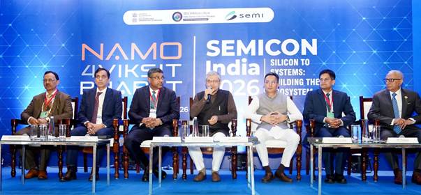
Image: the 17 September SEMICON media briefing, supplied by MeitY through PIB. This is event context, not a photograph of a design kit or regional facility.
Sources
Tags
More from Semiconductors
SEMICON India 2026 Opens in Delhi With Modi Inaugurating, 600+ Exhibitors
SEMICON India 2026, the fifth edition of the country's flagship chip-industry event, opens in New Delhi on September 17 with Prime Minister Modi inaugurating and more than 600 exhibitors taking part.
CDIL Confirms Commercial Chip Production, Partners With Japan's Shindengen on Packaging
Continental Device India Ltd (CDIL), one of India's oldest chipmakers, confirmed commercial-scale semiconductor production and a new packaging partnership with Japan's Shindengen Electric at SEMICON India 2026.