Paras Defence arm to build ₹6,200 crore advanced chip-packaging plant in Madhya Pradesh
Paras Defence''s subsidiary Paras Semiconductors has signed a ₹6,200 crore MoU with Madhya Pradesh to build a greenfield advanced OSAT chip-packaging plant near Ujjain-Indore, days after the Cabinet cleared India Semiconductor Mission 2.0.
Manik Gupta
Founder and editor of DeepTech India. Manik writes about India's frontier technology ecosystem — AI, semiconductors, space, quantum, robotics and biotech — translating research and policy into clear, reliable reporting.
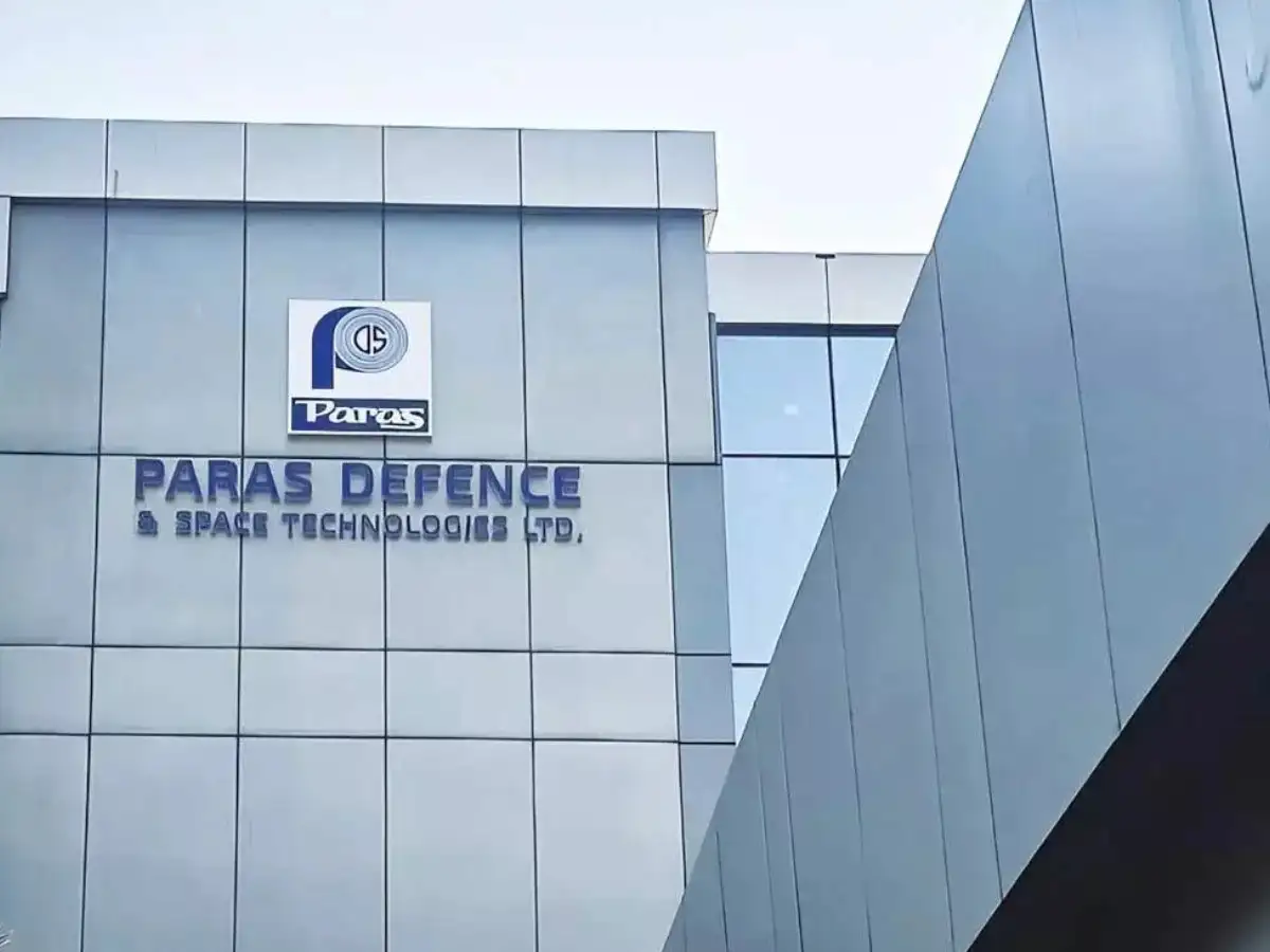
Paras Defence and Space Technologies has taken a sizeable step into semiconductors, with its subsidiary Paras Semiconductors signing a memorandum of understanding to set up a ₹6,200 crore advanced chip-packaging facility in Madhya Pradesh. The MoU, inked with the state's Department of Science and Technology on 22 July 2026, lands just a week after the Union Cabinet cleared the second phase of the India Semiconductor Mission — and signals that India's chip push is now reaching well beyond front-end fabrication.
Betting on the back end of the chip
Making a modern chip has two broad halves. The front end — the multi-billion-dollar wafer fabs that etch transistors onto silicon — gets most of the attention. The back end, known in the industry as OSAT (Outsourced Semiconductor Assembly and Test), is where those wafers are cut, packaged, connected and tested into the components that actually go into devices. It is less glamorous, but it is increasingly where a lot of the performance — and the value — of advanced chips is decided.
Paras Semiconductors is planting its flag firmly in that back end. The proposed greenfield facility is to be built on 50 acres allotted by the Madhya Pradesh government along the Ujjain–Indore corridor, and the company has laid out an unusually advanced technology roadmap for an Indian OSAT entrant.
An ambitious packaging menu
According to the company, the plant will undertake advanced packaging operations including 3D heterogeneous integration, 2.5D and 3D advanced packaging, hybrid bonding, ultra-high-density fan-out packaging, chiplet integration, wafer bumping, flip-chip assembly, and the associated testing and reliability work.
Those are not incremental techniques. Chiplet integration and hybrid bonding, in particular, are the methods the global industry is now using to keep improving chips as classic transistor scaling slows — stitching together multiple smaller dies into a single high-performance package. By naming them explicitly, Paras is positioning the facility toward the leading edge of packaging rather than commodity assembly, targeting the kind of high-value work that goes into AI accelerators, high-performance computing, defence electronics and communications hardware.
The project is expected to create around 2,500 jobs, and news of the MoU nudged Paras Defence's share price up on the day.
Riding the Semicon 2.0 wave
The timing is deliberate. The agreement comes just days after the Union Cabinet approved the second phase of the India Semiconductor Mission (ISM 2.0) on 15 July 2026, with an outlay of ₹1.275 lakh crore. Where the first phase concentrated on landing marquee fabrication and assembly investments, ISM 2.0 broadens government support across the whole ecosystem — chip design, advanced packaging, equipment, specialty materials, chemicals, research and talent.
Advanced packaging is one of the clearest beneficiaries of that broader mandate, and Paras's move reads as an early bet that state-level incentives and central support will now flow to companies willing to build capability in the back end of the chip supply chain.
From defence optics to silicon
For Paras Defence itself, the plan represents a significant diversification. The company is best known as a supplier of defence and space technologies — optics, electronics and systems for the armed forces — and a domestic chip-packaging business would extend it into the strategically sensitive semiconductor supply chain that underpins much of that same hardware.
There is a logic to that adjacency. Defence and space systems are voracious consumers of specialised, trusted electronics, and a sovereign packaging capability aligns neatly with India's stated goal of reducing dependence on imported chips for critical applications. Building in-house packaging expertise could, over time, give the group more control over the components that go into its own products.
The caveats
As with any MoU, the distance between signing and silicon is long. A ₹6,200 crore advanced-packaging plant is a multi-year undertaking that will require capital, equipment, process know-how and a workforce trained in some of the trickiest steps in chipmaking. Memoranda of understanding set intent; they do not by themselves pour concrete or qualify a single package.
Still, the announcement is a meaningful marker. It shows Indian firms moving up the semiconductor value chain into genuinely advanced packaging, it puts Madhya Pradesh on the country's chip map, and it suggests that ISM 2.0's wider net is already pulling in fresh, ambitious commitments. Whether Paras can execute on that ambition is the question the next few years will answer.
Sources
- Paras Defence to invest ₹6,200 cr to set up chip packaging facility in MP — Business Standard
- Paras Defence to set up semicon unit worth Rs 6,200 crore in Madhya Pradesh — The Week
- Paras Semiconductors to invest ₹6,200 cr in chip packaging facility in MP — Communications Today
- Paras Defence arm signs MoU worth ₹6,200 crore for semiconductor facility in MP — Upstox
Tags
More from Semiconductors
Makr Microsystems Raises ₹10.2 Crore to Help Chipmakers See What's Buried Beneath the Surface
Bengaluru's Makr Microsystems has raised ₹10.2 crore in a seed round led by Bluehill.VC to build nanoscale metrology tools that let chipmakers find hidden defects beneath a chip's surface without damaging it.
Zenergize Raises $4 Million to Scale India's First Indigenous Silicon-Carbide Power Electronics
Gurugram's Zenergize Technologies has raised a Pre-Series A round to scale its silicon-carbide EV chargers and solar inverters against an order book already worth ₹150 crore.